Single-sided PCBs are printed circuit boards that have conductive copper traces on only one side of the board. The conductive traces are etched or printed onto a single layer of non-conductive substrate material, typically fiberglass reinforced with epoxy resin (FR-4).
Key features and characteristics of single-sided PCBs include:
Single-sided PCBs are a cost-effective and straightforward solution for simpler electronic devices or applications where space and complexity requirements are minimal. While they have limitations in terms of component density and complexity, they remain relevant in various industries for specific purposes.
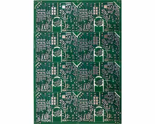
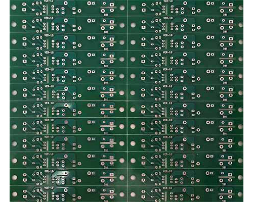
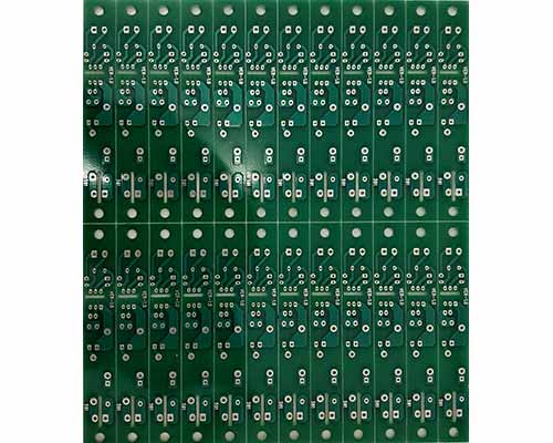
Our state of the art Single-sided manufacturing unit has been set-up recently which can delivery 7,500 m2 of Single-sided PCBs every month.
| Technical Specifications | Standard | Non-standard |
|---|---|---|
| Materials used | FR-4, FR4 (TG 180) | Ceramin, PTFE |
| Input Media | Gerber Data 274X, Gerber Data D, PCB File, DRL File | Gerber Data 274X, Gerber Data D, PCB File, DRL File |
| Approvals | IATF 16949:2016, UL94 - V0, ISO 9001:2015 | IATF 16949:2016, UL94 - V0, ISO 9001:2015 |
| Copper Thickness | 12 μ to 140 μ | Above 140 μ |
| Board Thickness | 0.30 mm to 3.20 mm | 0.30 mm to 3.20 mm |
| Minimum Hole Size (Finished) | 0.25 mm | 0.20 mm |
| Minimum Line Spacing | 0.15 mm | 0.125 mm |
| Minimum Line Width | 0.15 mm | 0.125 mm |
| Minimum Annular Ring | 0.10 mm | 0.075 mm |
| Maximum Panel Size | 1200 X 508 | 1200 X 508 |
| Minimum Solder Mask Dam | 0.15 mm | 0.10 mm |
| Hole Diameter Tolerence NPTH | +/-0.05 mm | +/-0.05 mm |
| Profile Routing Tolerence | +/-0.20 mm | ,+/-0.10 |
| Aspect ratio | 5.3:1 | 6.4:1 |
| Surface Finish | Lead Free HASL, Tin-lead HASL, and Lacquer | ENIG |
| Solder Mask Colors | Green, Black, White, Red, Yellow, Grey and Blue | All other colours |
| Peelable mask | Top, bottom or both sides | Top, bottom or both sides |
| Electrical test | 100% (Flying probe or fixture test) | 100% (Flying probe or fixture test) |
| Quality Standards | IPC-A-600 J / PERFAG | IPC-A-600 J / PERFAG |