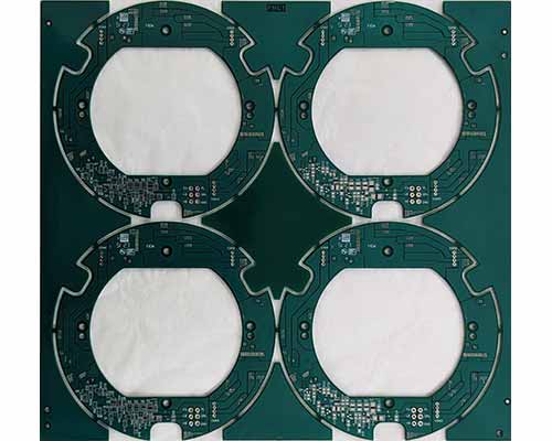
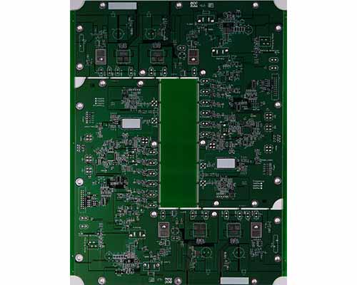
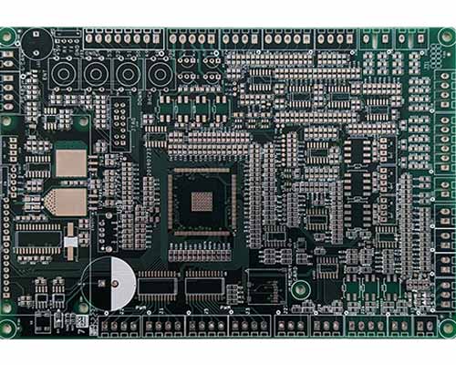
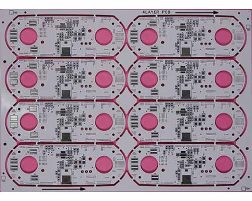
Multilayer PCBs are a type of printed circuit board that consists of more than two conductive copper layers (commonly four or more) separated by insulating layers, known as substrates or prepreg. These boards allow for more complex and denser circuitry compared to single or double-layer PCBs.
Here are some key aspects of multilayer PCBs:
In summary, multilayer PCBs offer increased design flexibility, improved performance, and higher integration capabilities, making them essential for many advanced electronic devices where space, performance, and complexity are critical factors.
BCC Fuba has been manufacturing and exporting multilayer PCBs since its inception and has the capability to manufacture PCBs up to 10 layers.
| Technical Specifications | Standard | Non-standard |
|---|---|---|
| Materials used | FR-4, FR4 (TG 180) | Ceramin, PTFE |
| Input Media | Gerber Data 274X, Gerber Data D, PCB File, DRL File | Gerber Data 274X, Gerber Data D, PCB File, DRL File |
| Approvals | IATF 16949:2016, UL94 - V0, ISO 9001:2015 | IATF 16949:2016, UL94 - V0, ISO 9001:2015 |
| Copper Thickness | 12 μ to 140 μ | Above 140 μ |
| Board Thickness | 0.30 mm to 3.20 mm | 3.2 mm to 4.5 mm |
| Minimum Hole Size (Finished) | 0.25 mm | 0.20 mm |
| Minimum Line Spacing | 0.15 mm | 0.125 mm |
| Minimum Line Width | 0.15 mm | 0.125 mm |
| Minimum Annular Ring | 0.10 mm | 0.075 mm |
| Maximum Panel Size | 535 X 406 | 560 X 450 |
| Minimum Solder Mask Dam | 0.15 mm | 0.10 mm |
| Hole Diameter Tolerence PTH | +/-0.075 mm | +/-0.05 mm |
| Hole Diameter Tolerence NPTH | +/-0.05 mm | +/-0.05 mm |
| Profile Routing Tolerence | +/-0.20 mm | ,+/-0.10 |
| Aspect ratio | 5.3:1 | 6.4:1 |
| Surface Finish | Lead Free HASL, Tin-lead HASL, and Lacquer | ENIG |
| Solder Mask Colors | Green, Black, White, Red, Yellow, Grey and Blue | All other colours |
| Peelable mask | Top, bottom or both sides | Top, bottom or both sides |
| Electrical test | 100% (Flying probe or fixture test) | 100% (Flying probe or fixture test) |
| Quality Standards | IPC-A-600 J / PERFAG | IPC-A-600 J / PERFAG |