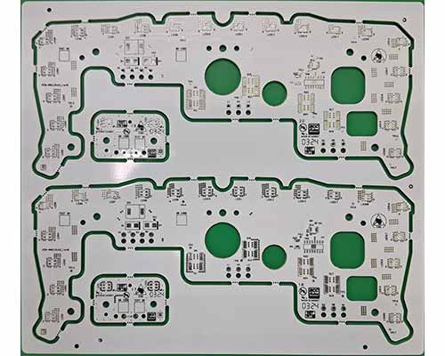
Double-sided PCBs, also known as two-layer PCBs, are a type of printed circuit board that has conductive copper traces on both the top and bottom layers of the board. These layers are separated by an insulating layer (typically made of a substrate material like fiberglass reinforced with epoxy resin, known as FR-4).
Key features and characteristics of double-sided PCBs include:
Double-sided PCBs strike a balance between complexity, cost-effectiveness, and functionality, making them a popular choice for a wide range of electronic applications where a moderate level of circuit complexity and component density is required.
Our Double-sided PCB manufacturing unit has a capacity to delivery 6,000 m2 of Double-sided PCBs every month.
| Technical Specifications | Standard | Non-standard |
|---|---|---|
| Materials used | FR-4, FR4 (TG 180) | Ceramin, PTFE |
| Input Media | Gerber Data 274X, Gerber Data D, PCB File, DRL File | Gerber Data 274X, Gerber Data D, PCB File, DRL File |
| Approvals | IATF 16949:2016, UL94 - V0, ISO 9001:2015 | IATF 16949:2016, UL94 - V0, ISO 9001:2015 |
| Copper Thickness | 12 μ to 140 μ | Above 140 μ |
| Board Thickness | 0.30 mm to 3.20 mm | 0.30 mm to 3.20 mm |
| Minimum Hole Size (Finished) | 0.25 mm | 0.20 mm |
| Minimum Line Spacing | 0.15 mm | 0.125 mm |
| Minimum Line Width | 0.15 mm | 0.125 mm |
| Minimum Annular Ring | 0.10 mm | 0.075 mm |
| Maximum Panel Size | 600 X 508 | 820 X 508 |
| Minimum Solder Mask Dam | 0.15 mm | 0.10 mm |
| Hole Diameter Tolerence PTH | +/-0.075 mm | +/-0.05 mm |
| Hole Diameter Tolerence NPTH | +/-0.05 mm | +/-0.05 mm |
| Profile Routing Tolerence | +/-0.20 mm | ,+/-0.10 |
| Aspect ratio | 5.3:1 | 6.4:1 |
| Surface Finish | Lead Free HASL, Tin-lead HASL, and Lacquer | ENIG |
| Solder Mask Colors | Green, Black, White, Red, Yellow, Grey and Blue | All other colours |
| Peelable mask | Top, bottom or both sides | Top, bottom or both sides |
| Electrical test | 100% (Flying probe or fixture test) | 100% (Flying probe or fixture test) |
| Quality Standards | IPC-A-600 J / PERFAG | IPC-A-600 J / PERFAG |